

Cadence Tools Support Hotline
(+60) 1111 247 265
 Product Details
SiP layout options
SiP layout options enhance Cadence Allegro ® The constraints and rules of X Package Designer drive the layout environment to design high-performance and complex packaging technologies. It adds a powerful set of automated workflow, routing, and adjustment functions, accelerating the planning, optimization, instantiation, and timing convergence of critical interconnects such as DDR memory, high-speed serial, silicon substrate, and graphics interfaces. Intelligent wiring process planning and automatic grouping tools reduce time-consuming and tedious manual grouping and wiring tasks, and optimize large bus wiring to use minimal space and layers. The SiP layout option also adds additional automatic routing functionality based on Specctra technology to silicon-based substrates.
The comprehensive Allegro X PCB Design True DFM Technology and assembly rules have increased substrate production and prevented manufacturing and assembly issues. This option supports evaluating manufacturing changes and creating design changes with different substrate stacking, die stacking, and wire bonding configurations, which can be provided by the same main design. This option also enables bidirectional flow with the Virtuoso platform for collaborative design of IC/encapsulation.
Advantage
➤ Based on signal integrity and distributability, it allows for connection allocation and optimization between ICs, components, and substrates to minimize the use of layers
➤ Includes comprehensive substrate manufacturing design (DFM) capabilities for rapid manufacturing preparation
➤ Create bonding and stacking variants from basic design; Evaluate the impact of process changes (such as line width) on design rule checks and system performance
Function
Interface aware design
In advanced packaging design, in order to meet product performance, power, and bandwidth requirements, you may need to switch to protocols such as DDRx, HBM, graphics, and high-speed serial bus. And can your layout tool provide fast and easy-to-use performance to meet the requirements of the design cycle? What if you could use a layered interface aware approach to accelerate the implementation process and improve design quality, performance, and reliability during that time?
The interface aware design feature allows you to design packaging in a more abstract way, allowing for faster routing on standard based interfaces. Traditional design creation tools combine buses or wiring harnesses with single level hierarchical definition of a set of signals. However, the current interface cannot be modeled in a single level hierarchical structure. Other challenges that need to be addressed include an increase in the number of constraints, an increase in design density, a reduction in bump and pillar spacing due to an increase in the number of large pin devices, and an increase in wiring design time (facing a reduction in design cycle time and resources).
In order to quickly and conveniently establish connections with interfaces, the layered interface aware design feature in SiP layout options:
Through this' workflow ', we can help you achieve functions including instantiation of interfaces and hierarchical network groups, configuring interfaces and connecting them with components and blocks, allocating layout layers, and exchanging allocations for distributable lines and escaping.
Automatic interaction&automatic routing
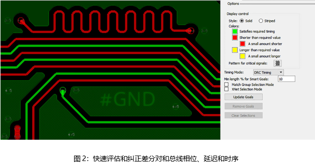
The SiP layout option adds a complete set of automatic interaction functions, which can quickly design complex and critical interconnects such as high-speed interfaces and buses in IC packaging design. It provides tools for planning and grouping convex blocks and spherical patterns on molds. The attached tools can also solve the timing, delay, and phase adjustment problems of bus components, provide visual warnings where problems occur, and offer means to correct them. The automatic routing function based on Specctra includes applications for casting and silicon-based substrates. These features reduce tedious, time-consuming, and manual group editing and linking.
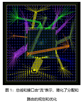
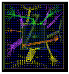
Figure 1: Buses and interfaces are represented by "flows", simplifying the planning and optimization of allocation and routing
Allegro X Package Designer integrates a real-time high-level language rule checking engine that eliminates the tedious traditional post design manufacturing mask checking. This engine can greatly shorten the manufacturing preparation time, simplify the design process, and enhance the capability of packaging design tools. Custom DRC rules can also be written and encrypted using optional rule developer toolkits.
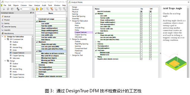
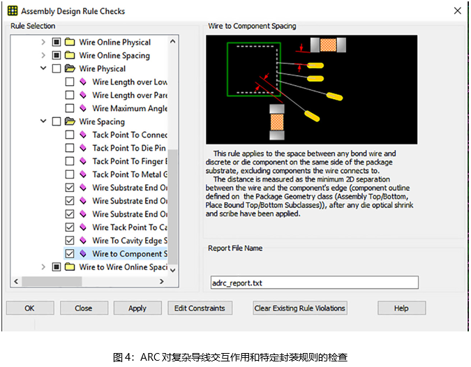
The SiP layout option adds a comprehensive assembly (and manufacturing) rule checker (ARC), providing over 50 unique package IC inspections, including complex line spacing and crossing rules. Inspections can be performed individually as a single inspection group or as a custom selection; The results will be displayed in the Constraint Manager DRC tab, DRC browser, and highlighted graphically in the design. Similarly, this option can increase substrate yield and prevent issues caused by manufacturing and assembly through a complete set of Design True DFM rules. The DesignTrue DFM technology can help you design for the sake of craftsmanship, rather than redesigning for the sake of craftsmanship or frequently modifying craftsmanship, while accelerating the launch of new products. You can define manufacturing rules before starting the design and apply them in real-time to your design. When you complete the design, you are ready for the first round of DFM validation.
Craftsmanship rules are easy to manage and collaborate on. Like electrical constraints, an easy-to-use spreadsheet interface is very intuitive for both engineers and non engineers, making it easy to reuse. Constraints have a highly configurable ability to enable and disable groups, entire rule categories, or individual rules. The rules can be applied to etching mode, non etching mode, and stacking mode, allowing designers to isolate layers, geometries, and notches.
Figure 2: Rapid evaluation and correction of differential pairs and bus phase, delay, and timing
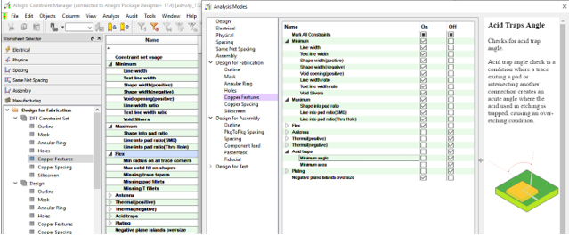
Figure 3: Checking the Craftsmanship of Design through Design True DFM Technology
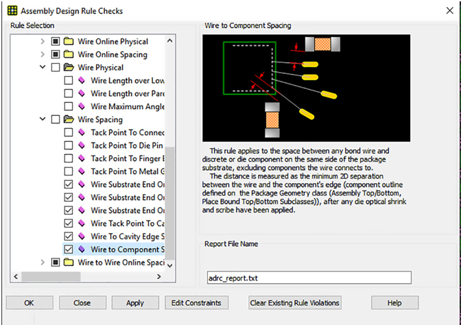
Figure 4: ARC inspection of complex wire interactions and specific encapsulation rules
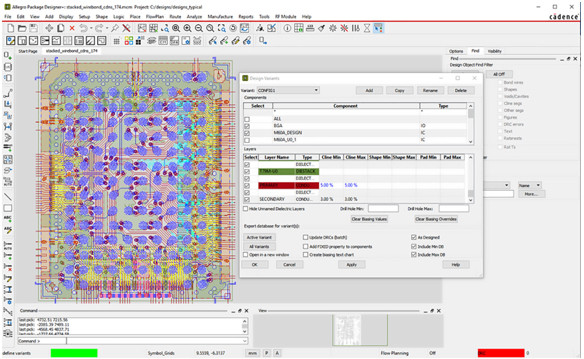
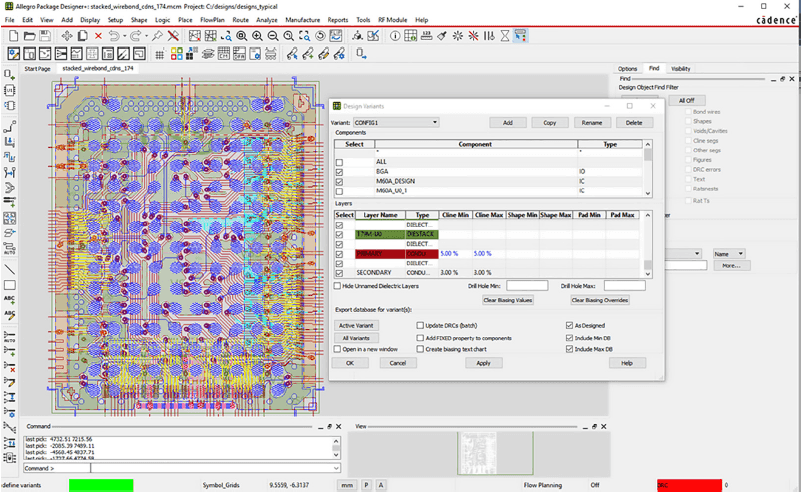
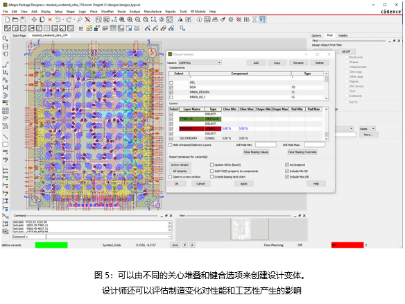
Figure 5: Design variants can be created using different stacking and bonding options, and designers can also evaluate the impact of manufacturing changes on performance and processability
Design and process variations
A package substrate design typically has multiple configurations, including die components and stack variations, or die bonding methods. The SiP layout option allows designers to create a main design, generate sub coordinate designs representing each variant, and then evaluate different bonding and stacking option designs for physical DRC, wire DRC, and signal integrity. Similarly, this option supports in house manufacturing variant evaluation for DRC and signal integrity.
Success Cases

