

Cadence Tools Support Hotline
(+60) 1111 247 265
 Product Details
◆ Automate the selection and placement of decaps
◆ Eliminate decap over-design for PCBs and IC packages
◆ Reduce PDN cost of new designs and postproduction products
◆ Recapture design area used by unnecessary decaps
◆ Develop effective decap design guidelines
◆ Investigate pre-layout decap placement and selection scenarios
◆ Interactively assess tradeoffs for PDN cost vs. performance
◆ Understand both system- and device-level PDN performance
◆ Create lowest-cost, best performance decap placement tables
◆ Capture Cadence Allegro PowerTree data from schematic data and visualize the PDN topologies
◆ Automatically set-up post route analysis using PowerTree data captured during the logical design stage of PCB design
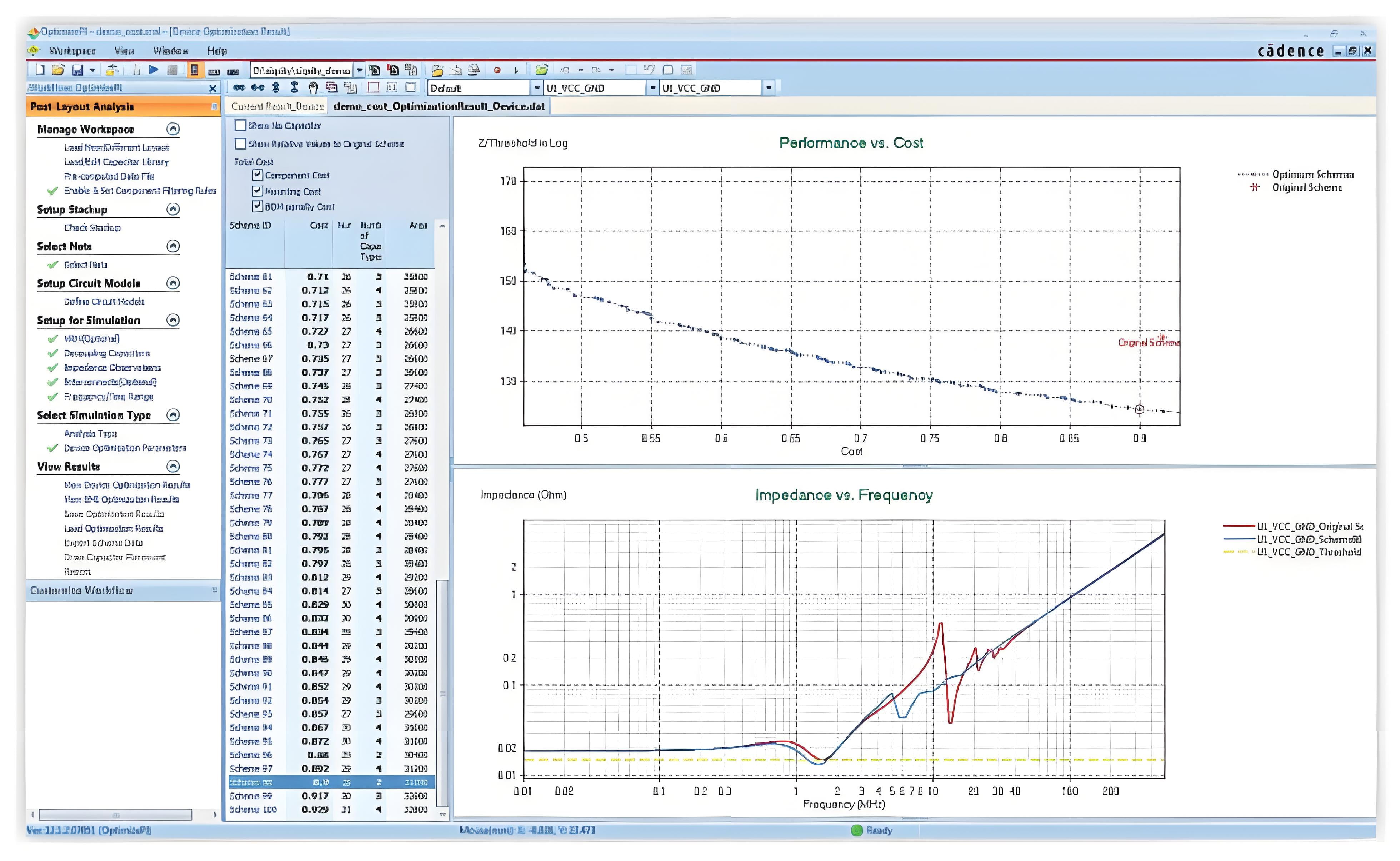
Decap cost savings of 15% to 50% are typical with the Sigrity OptimizePI environment. Designs with a large number of decap components and those manufactured in volume benefit most. Cost savings are achieved by reducing the number of decaps placed and by targeting lower-priced components where practical. Device suppliers may suggest general guidelines such as “one decap per power pin” or describe preferred decap implementation schemes. Both approaches typically lead to an overly robust system. The Sigrity OptimizePI approach helps companies capitalize on this margin to gain market advantage.
The Sigrity OptimizePI tool’s cost savings are achieved while analytically assuring PDN performance.
Alternatively, the Sigrity OptimizePI tool may be configured to maximize performance or reduce decap area without regard for cost. Complex interactions among performance, decap selection, component cost, and placement expense are considered. The Sigrity OptimizePI design schemes are the best-performing alternatives from all feasible designs. Analysis results are based on aggregate PDN performance averaged across frequency. Users can set device-specific targets and identify critical frequencies for further refinement. Time-domain results confirmation is also included.
Figure 1: Sigrity OptimizePI capabilities quickly pinpoint designs that offer the same or better performance at lower cost
While primarily targeting post-layout PDN optimization, pre-layout design scenarios can also be explored. This helps to eliminate decap over-design earlier in the design flow and supports development of analytically based decap placement design guides for individual devices. While the design is being implemented, PowerTree information, captured during the design’s logical design (schematic) stage, can be called on to simulate individual power rails as they are developed. Because the simulation set-up will be automated, either the layout designer or PI engineer can validate that target impedance constraints are being met as an in-design task. For post-layout applications, the Sigrity OptimizePI approach works from an initial design imported from a layout database. Sigrity OptimizePI capabilities can also be applied by manufacturing engineers for postproduction cost reduction. The optimized decoupling scheme can be automatically updated in Cadence PCB design tools.
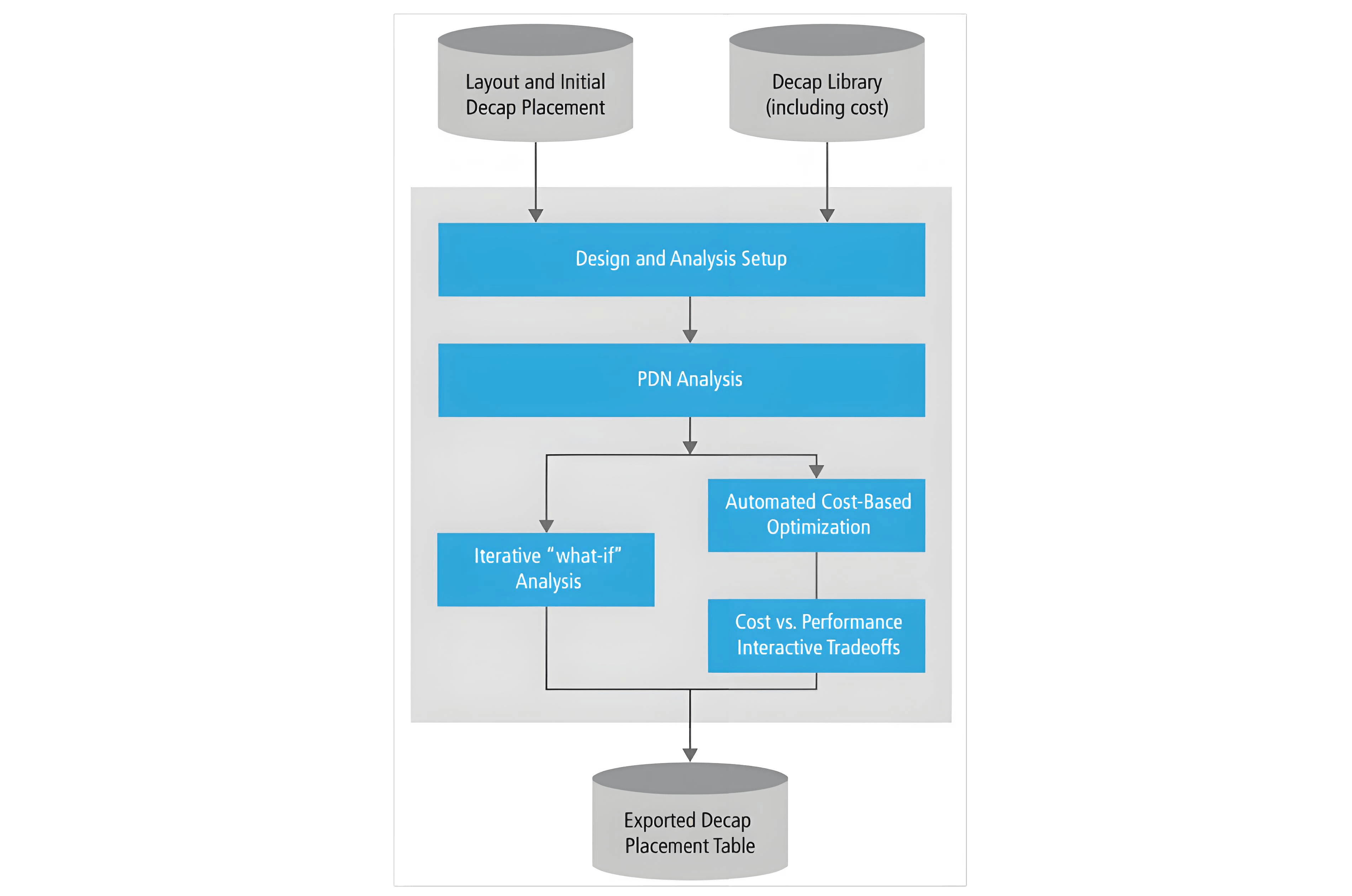
Figure 2: A Sigrity OptimizePI workflow for a post-layout optimization
Setting up a design in the Sigrity OptimizePI environment typically requires less than 30 minutes of engineering time. Users are guided step by step through each task in the workflow. Initial set-up involves importing the PCB or IC package design and identification of an Sigrity OptimizePI library corresponding to a corporate decap preferred parts list. Decap component and placement costs are included in this library along with vendor-supplied electrical models. Set-up options enable decap selection filtering, biasing the importance of a device to overall PDN performance, and so on. Individual decap selections may be limited to a subset of the library or restricted by decap size. An interactive results window enables exploration of alternate design schemes. The Sigrity OptimizePI results can be exported to a spreadsheet for back annotation to the layout system.
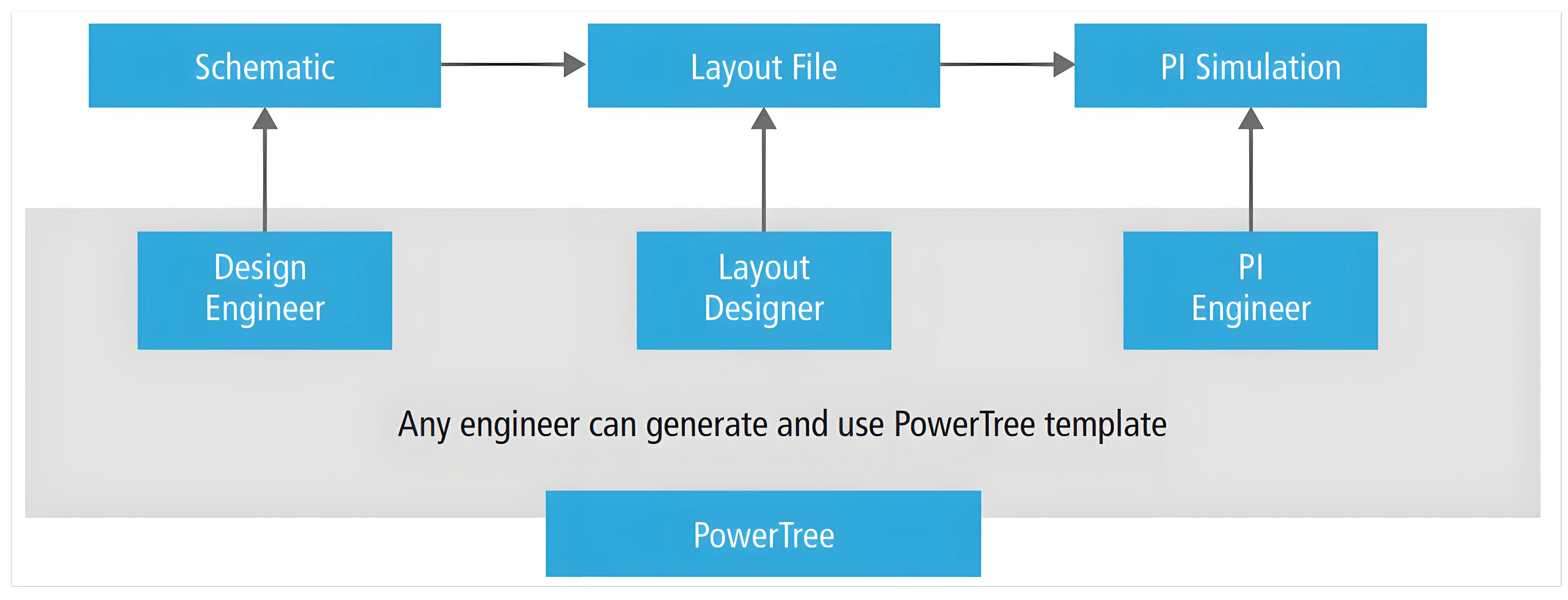
Figure 3: PowerTree technology enables the design engineer to have early visualization and define simulation criteria to ensure the layout designer’s decap placement and PDN design meets target impedance requirements for each power rail on each component.
◆ Works with Microsoft Windows and Linux with multi-processor support
◆ Interfaces to PCB and IC package layout databases from Cadence, Mentor Graphics, Altium, Zuken, etc.
Success Cases

