

Cadence Tools Support Hotline
(+60) 1111 247 265

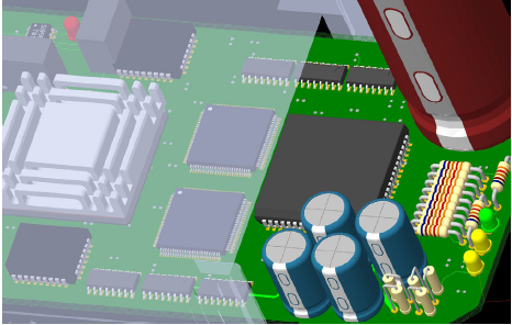
OrCAD ® The X PCB design solution meets all the needs of users in PCB design, from concept to product. In any EDA industry, scalability and product performance improvement are representative. Faced with many challenges such as shorter design cycles, increasingly tight project requirements, and faster time to market in current design, OrCAD X PCB Designer Standard and OrCAD X PCB Designer Professional enable enterprises to maintain competitiveness in the electronics industry.
 Product Details
OrCAD X PCB products provide a hierarchical and scalable PCB design solution, offering powerful performance and highly integrated design processes. Whether the user's PCB design is simple or complex, such as high-density, complex rules, mixed signal circuits, standard circuit interfaces, OrCAD X's PCB solutions can help companies improve team productivity and efficiency, reduce cost waste, and shorten time to market.
The OrCAD X PCB solution can not only meet your special design needs, but also meet your budget. Investing in low-cost design input tools for you
最小化。Orcad X PCB 是强大,高集成度的PCB设计解决方案,包括原理图、库工具、PCB编辑/走线、约束管理器,信号完整性(Professional)、自动布线(Professional)以及可选的混合信号电路仿真模块。软件易用、直观并且在升级到Cadence Allegro系列产品上市,早期设计文件也可以是实现平滑的过渡。
Based on the same data architecture, using models and library files, the OrCAD X PCB design solution is fully compatible with OrCAD X and Allegro X PCB solutions. It is easy to expand from OrCAD X platform to Allegro X platform when facing higher design challenges.
Product Highlights
➤A validated, scalable, and easy-to-use PCB editing and routing solution that continuously develops new features as design complexity and demand increase.
➤A complete design solution with highly integrated and rich functional features, completing the entire PCB design process from concept to product, improving productivity and ensuring data integrity.
➤The constraint manager provides real-time inspection and status display of physical rules/spacing rules, same network rules, region rules, differential pair rules, length constraints, and other rules, helping users improve the success rate of a design.
➤Combining automatic and interactive layout and routing to achieve intelligent automation operations, ensuring user control while maximizing productivity.
➤Dynamic copper technology provides real-time avoidance and copper filling, reducing manual avoidance and repetitive labor that are prone to errors
➤Supports IPC-2581, STEP, and IDX. Provide intelligent and seamlessly integrated MCAD-ECAD design process.
Layout and wiring functions
The core tool of OrCAD X PCB solution, OrCAD X PCB Editor, is a design environment that integrates usability and interactive layout and routing functions for creating and editing PCBs from simple to complex. Its rich functional features can meet the challenges of the latest designs and manufacturability. These powerful and flexible features include automation, schematic driven pre layout and interactive layout, intelligent interactive routing, dynamic copper laying, layout reuse, simple and advanced rules (including differential pairs, length, area, layer, etc.), STEP model support and 3D view, MCAD-ECAD (interface for manufacturing and mechanical CAD), etc.
Pre layout and placement
The automatic, schematic driven pre layout and interactive layout functions are used to accelerate the progress of the layout phase. In the schematic input stage, specify the device or sub circuit as a specific "Room" to achieve automatic pre layout. In interactive layout mode, devices can be filtered and selected in various ways, such as by tag number, encapsulation, network name, device number, or schematic page.
Interactive Routing
文档
图片
277/10000
实时翻译
The interactive cabling function provides controllable automation capabilities to maximize routing efficiency. The real-time, shape based, and arbitrary angle pushing of routing is sufficient to address most routing challenges. The routing engine optimizes routing by pushing obstacles or skipping obstacles encountered when encountering vias or device pins, and routing along the contour of the obstacles. There are three wiring modes, including "push first", "surround first", and "surround only". In the push first routing mode, the routing engine searches for the optimal path by pushing or jumping over obstacles encountered on the routing path. The surround first wiring mode should be the preferred choice when constructing the physical routing of the bus. In this mode, the routing only follows the contour of another routing, and only chooses to push the adjacent routing or jump over obstacles if it cannot be routed.
Dynamic copper laying
The dynamic copper laying technology provides real-time dynamic avoidance and copper pouring functions, and the properties of copper laying can be assigned to three different levels: global, copper laying instance, and object level. When adding wires, vias, and devices, the copper foil will automatically avoid them, and when deleting them, the copper foil will also automatically backfill the original avoidance area. Dynamic copper laying does not require batch style automatic avoidance or other post-processing steps after editing.
Copy and reuse of layout
Intelligent layout reuse technology enables users to automatically reuse layouts and wiring from a source module in the design. If you want to make changes to all modules, simply change the layout or routing of the source module to automatically update it to other reusable modules. Some validated circuit templates can reuse layout and routing to other devices.
Constraint Manager
Design rules, electrical, and physical constraints are more important than ever for the success of your product design. For today's design, in order to cope with these complex rules and constraints, a powerful constraint management system is needed that can cover all aspects from constraint creation, management to inspection and verification. OrCAD X PCB Constraint Manager displays physical/spacing, same network, region, differential pairs, line length, and other rules, as well as the rule status based on current design data throughout the entire PCB design process. Each worksheet provides form data with different constraints, making it easy to define, manage, and perform hierarchical validation of rules. The constraint manager OrCAD X PCB is fully integrated, and specific constraints can also be checked in real-time during the design process, and whether they pass the rule check can be displayed graphically (highlighted in green, not in red). This method allows users to see the real-time status of constraint rules in the design in the constraint manager, and the status of modifications made to the project can also be seen immediately.
3D Display and View
The OrCAD X 3D view environment allows users to view a realistic 3D view of the PCB, where several filtering options can be applied, such as solid fill, transparency, and wireframe display. The 3D view also supports the display of complex via structures and PCB partial views, in order to display more details. OrCAD X PCB supports importing models in STEP format for more precise display of components and mechanical objects, such as casings, which can be viewed in the current PCB view. This feature allows designers to check for device overlap and avoid errors in device position conflicts before production.
PCB manufacturing
OrCAD X PCB design solution supports the output and testing of a complete set of optical drawing files and bare board manufacturing files. The output supports Gerber 274x, NC drill, and multiple formats of bare board testing files. OrCAD X PCB supports industrial oriented Gerber free manufacturing file output and export in IPC-2581 format. IPC-2581 provides precise and highly reliable manufacturing data for high-quality manufacturing in a single file. Users can also choose to export some data to protect intellectual property rights.
Design solutions and processes
Layout signal integrity analysis
OrCAD X PCB Professional supports extracting both wired and unpaired network topologies for simulation to verify whether the PCB meets the requirements. Topology extraction can be performed in three key stages of design for signal quality analysis: layout stage, routing stage for key signals, and after wiring is completed. Topology extraction, network analysis, and comparison between simulation results before or after wiring and expected performance are all completed in the same interface. The topology extracted after wiring includes detailed electrical information, such as the actual physical connections of the network, layered structure, wiring layers, via models, routing lengths, etc. If the analysis results do not match expectations, the PCB needs to be modified for further analysis.
ECAD-MCAD Collaborative Design
The ECAD-MACD collaborative design in OrCAD X PCB solution uses the IDX file format, allowing users to make incremental engineering changes synchronously between electrical and mechanical design environments. Unlike intermediate file formats IDF or DXF, IDX format allows users to preview and analyze data changes in the form of images before receiving or rejecting data. Moreover, in both environments, designers can choose to accept or reject data changes object by object, or provide other change suggestions. This interactive approach provides an unprecedented level of control and collaboration, ensuring data synchronization between the two design environments. This feature also helps designers avoid communication errors that lead to repetitive work, and greatly improves the success rate of product design in one go.
Automatic wiring
OrCAD X PCB Designer Professional is highly integrated with Cadence SPECCTRA, a leading interactive automatic routing tool in the PCB industry. SPECCTRA automatic routing tool is used to solve the challenges of automatic routing from simple PCBs to high-density PCBs with high complexity constraint rules. OrCAD X SPECCTRA utilizes powerful algorithms to maximize the efficiency of wiring space. Increase the step rate of wiring, improve productivity, and shorten the design and manufacturing cycle. OrCAD X SPECCTRA provides two interactive routing tools: a routing editor and an automatic routing tool, which control various routing constraints through a large number of rule settings.
Success Cases

