Benefits
Use PowerSI to:
Establish power delivery system (PDS) and SI guidelines
Extract fully coupled electrical models of signal, power, and ground networks in IC packages and PCBs for use in time domain simulation of simultaneous switching noise
Fully assess decoupling capacitor strategies and verify placement effects
Evaluate electromagnetic coupling between geometries (planes, traces, and vias)
Extract frequency-dependent impedances or S-parameters directly from PCB, package, and SiP layout data
Anticipate energy leaks with nearand far-field radiation display to reduce downstream electromagnetic interference (EMI)/electromagnetic capability (EMC) challenges
Analyze PDS cavity resonance
Perform DC analysis
Create broadband SPICE models for packages and PCBs with the Sigrity Broadband SPICE option
Advanced Analysis Techniques
Fast and accurate
PowerSI efficient electromagnetic analysis techniques are ideal for modeling entire PCBs or IC packages with full-wave accuracy. PowerSI speed stems from unique patented methodologies that allow for autoadaptive numerical meshes, enabling accurate modeling for complex structures such as cuts and slots in planes, multiple power and ground layers, and any number of vias and traces. PowerSI intelligent multi-processor support distributes simulations for the fastest possible throughput. With an optional high-performance computing license, simulations can be distributed across multiple machines to further enhance throughput. With the PowerSI approach, designers can fully analyze and strategically tune their designs to achieve performance and schedule objectives.

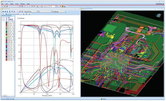
Figure 1: 3D view of system-level design including IC package and PCB for PDS analysis and SI verification
Comprehensive analysis
Unlike traditional SI tools that treat power and ground planes as ideal with fixed voltages, the PowerSI approach fully considers all signal and plane effects simultaneously. This is achieved in an environment that provides a high degree of automation. With the PowerSI approach, there is no need to segment designs before simulation. This eliminates cumbersome design preparation while also offering greater accuracy than evaluating a system a few components at a time, as required by approaches relying on traditional 3D analysis.
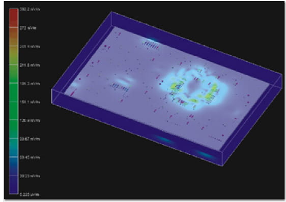
Figure 2: PowerSI display of board-level near-filed emissions
Flexible Workflow
In Extraction mode, the PowerSI environment provides a convenient way to extract S, Z, and Y parameters of userselected ports. With simulations in Spatial mode, the PowerSI approach facilitates AC analysis to assess voltage distribution across ground planes. Users can flexibly control observation locations to focus on areas of interest such as voltage levels between plane pairs and performance for specific frequency ranges. A variety of 2D and 3D visualization options enables rapid results assessment. PowerSI capabilities incorporate a task-focused workflow that can be customized to provide step-by-step guidance tuned for frequent analysis tasks and to establish defaults to guide new users.
Proven Capability
Designs today are called on to create quality products at the lowest possible cost. The PowerSI environment enables early issue detection and streamlines resolution. Early visibility into potential EMI issues complements PI and SI capabilities. Near- and far-field radiation is displayed along with 3D geometry information. With the PowerSI approach, designers can fully analyze and strategically tune their designs to increase market advantage, which is why the Sigrity advanced SI and PI solutions are used by nearly every major electronics company in the world.
Integration
Works with Microsoft Windows and Linux with multi-processor support
Interfaces to PCB and IC package layout databases from Cadence, Mentor Graphics, Altium, Zuken, etc.
Supports circuit models in SPICE format


 Product Details


 Success Cases