

Cadence Tools Support Hotline
(+60) 1111 247 265
Although wafer level packaging (WLP) is not a new technology or process, like all technologies, it is constantly evolving. As the latest development of FOWLP driven by casting, it provides many new advantages for the segmented markets of handheld, mobile, wireless, and multimedia products.
FOWLP technology is based on wafer forming and substrate free fine metal processes, and is an ideal choice for reducing thickness, optimizing performance, and lowering costs to achieve the initial target market (mobile computing products such as smartphones and tablets). With the emergence of faster and more powerful multi-core application processors, these devices are gradually developing rapidly. Compared to traditional chip level packaging methods, FOWLP can achieve thinner PoP stacks, better wiring density, higher operating frequency (maximum frequency (f MAX)), DRAM with higher memory bandwidth, and better heat dissipation performance.
 Product Details
Most of the emerging FOWLP designs are typically handled by the IC backend design teams of fabless semiconductor companies. However, these designs also have certain requirements for IC packaging substrate designers or teams - IC packaging design tools must be able to expand to meet the requirements of modern FOWLP design. By collaborating with leaders in this emerging field, Cadence has developed silicon layout options that provide a complete design validation process for FOWLP's specific design and manufacturing challenges.
Due to the wafer level implementation and process of silicon layout options, the manufacturing path and typical organic substrate based IC packaging manufacturing process are completely different. For silicon layout options, the manufacturing process and IC manufacturing process are the same or very similar. At the macro level, the differences and challenges compared to traditional organic IC packaging manufacturing include:
➤ Process Design Kit/Rule Platform (PDK) must be used and verified for retesting
➤ Specific interconnects (metal) must follow common casting/manufacturer rules and techniques in IC design and manufacturing
➤ GDSII or Stream is a mask creation path used for FOWLP manufacturing
➤ PDK compliance verification/re inspection is required before the design/mask enters the manufacturing process

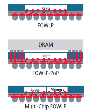
Figure 1 FOWLP Example
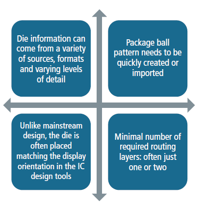

Figure 2: Some typical design challenges unique to FOWLP implementation must be addressed by design tools and designers
PRODUCT FUNCTION
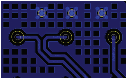

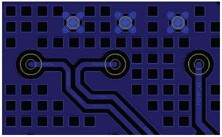
Figure 3: The metal creation and management tool allows designers to scan, evaluate, and modify the local metal density of each layer to meet the strict manufacturing requirements of the foundry for copper foil and solder pads
The combination of silicon layout options and Cadence Physical Verification System (PVS) enables designers to handle these macro level projects. Some of its specific functions include:
➤ A creation and editing tool that can localize and strictly control metal density, and can control the bending of ultra-thin packages (500 to 1000 µ m)
➤ A metal density utility for cross design balancing of mesh metals and mesh substrates
➤ High performance GDSII mask processing
➤ Options are directly integrated with PVS for design and mask validation, as well as retesting of PDK rules
➤ Report and highlight PVS validation issues directly in the design canvas and constraint manager

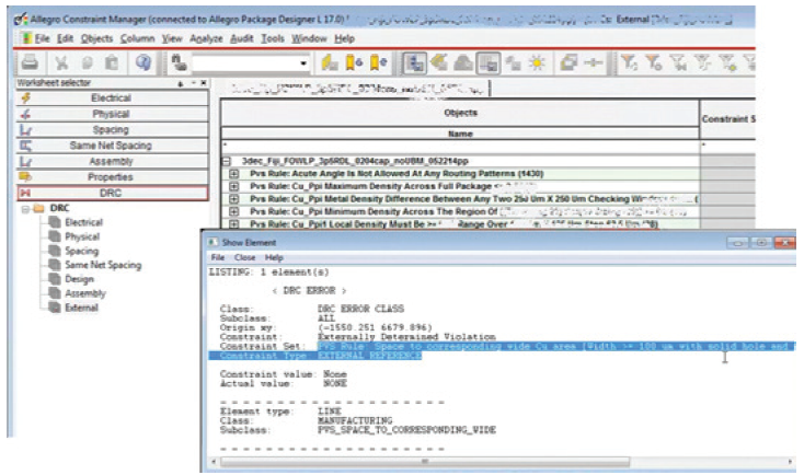
Figure 4: PVS validation results driven by PDK/rule groups provided by the foundry, displayed directly using the SiP editor of the constraint manager
Success Cases

